Introduction
Precision, efficiency, and reliability are paramount In the realm of electronics manufacturing. Two cornerstone techniques that stand out in the assembly of printed circuit boards (PCBs) are through-hole component insertion and wave soldering. These processes exemplify technological advancement and reflect the industry's commitment to quality and efficiency.
The Significance of Through-Hole Components Insertion and Wave Soldering
Through-hole component insertion and wave soldering are crucial for creating durable and reliable electronic assemblies. While surface-mount technology (SMT) has gained prominence for its miniaturization capabilities, through-hole mounting remains unbeatable for high-reliability applications requiring strong mechanical bonds. The synergy of these techniques offers a comprehensive solution for assembling complex electronic circuits.
Through-Hole Components Insertion: The Foundation of Electronic Assemblies
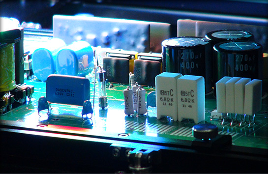
Through-hole technology (THT) involves inserting components with leads into drilled holes on a PCB. This method is favored for its mechanical solid bonds and excellent electrical connections, making it ideal for stressed components or needing high power.
The Process:
Preparation
Before insertion, the PCB is prepared with all necessary holes drilled according to the component leads' specifications.
Insertion
Components are inserted manually or with automated machines, ensuring correct orientation and placement.
Inspection
Inserted components are inspected for alignment and correct placement before soldering. This technique is pivotal for components that require robust physical connections, offering superior durability and reliability over surface-mounted parts.
Wave Soldering: Streamlining PCB Assembly
Wave soldering is an automated soldering process used to attach electronic components to the PCB. It involves passing the assembled board over a pan of molten solder; a pump creates a wave of solder that washes over the board, soldering the component leads to the PCB.
The Process:
Flux Application
Flux is applied to the PCB to clean and prepare the metal surfaces for soldering, ensuring a strong bond.
Preheating
The PCB undergoes preheating to avoid thermal shock and improve solder flow.
Soldering
The board is passed over the wave of molten solder, allowing the solder to flow into the joints between the component leads and the PCB.
Cooling and Cleaning
After soldering, the board is cooled and cleaned to remove any flux residues.
Wave soldering is renowned for its speed and efficiency, capable of soldering multiple boards in a fraction of the time required for manual soldering.
Comparing Techniques
While both through-hole insertion and wave soldering are integral to PCB assembly, they serve different purposes. Through-hole insertion provides the mechanical strength needed for components that undergo physical stress. In contrast, wave soldering offers a fast and efficient method for creating solder joints on a large scale.
Best Practices and Considerations:
Design Considerations
Optimze PCB design for through-hole components to facilitate easy insertion and wave soldering.
Quality Control
Implement rigorous inspection protocols to ensure high-quality solder joints and correct component placement.
Environmental Factors
Consider lead-free solder options and other environmentally friendly materials to align with global standards and regulations.
Conclusion
The combination of through-hole component insertion and wave soldering represents a balanced approach to PCS assembly, marrying the robustness of through-hole connections with efficiency of wave soldering. As technology evolves, these time-tested techniques continue to play a crucial role in manufacturing reliable and high-quality electronic products.